News Highlights:
- UMC's 3D IC solution for RFSOI reduces circuit footprint by more than 45%, enabling integration of more RF components in 5G-enabled devices.
- UMC's innovative 3D IC technology addresses the challenge of radio frequency (RF) interference, and the company also seeks to develop 3D IC solutions for 5G mmWave going forward.
- UMC's comprehensive solutions for RF front-end modules are available in various technology types and technology nodes, delivering unparalleled performance.
United Microelectronics Corporation (NYSE: UMC; TWSE: 2303) (“UMC”), a leading global semiconductor foundry, today announced the industry’s first 3D IC solution for RFSOI technology. Available on UMC’s 55nm RFSOI platform, the stacked silicon technology reduces die size by more than 45% without any degradation of radio frequency (RF) performance, enabling customers to efficiently integrate more RF components to address the greater bandwidth requirements of 5G.
This press release features multimedia. View the full release here: https://www.businesswire.com/news/home/20240501611964/en/
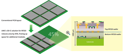
UMC's 3D IC solution for RFSOI reduces area by 45%, freeing up space for additional modules (Graphic: Business Wire)
As mobile device manufacturers pack more frequency bands in newer generations of smartphones, the company’s 3D IC solution for RFSOI addresses the challenge of integrating more RF front-end modules (RF-FEM) - critical components in devices to transmit and receive data – in a device by vertically stacking dies to reduce surface area. RFSOI is the foundry process used for RF chips such as low noise amplifiers, switches, and antenna tuners. Utilizing wafer-to-wafer bonding technology, UMC’s 3D IC solution for RFSOI resolves the common issue of RF interference between stacked dies. The company has received multiple patents for this process, which is now ready for production.
“We are proud to lead the industry in offering this state-of-the-art solution utilizing our innovative 3D IC technology for RF-FEM. This groundbreaking technology not only solves the challenges of increased frequency band demands in smartphones in the 5G/6G era, but also helps in mobile, IoT, and virtual reality devices with faster data transfer by accommodating more frequency bands in parallel,” said Raj Verma, Associate Vice President of Technology Development at UMC. “We are excited to continue developing stacked die solutions to meet our customers’ RF needs, such as for 5G millimeter-wave, in the future.”
UMC offers the most comprehensive RF front-end module IC solutions in the industry, catering to a broad range of applications including mobile, Wi-Fi, automotive, IoT, and satellite communications. With over 500 product tape-outs completed and more than 38 billion RFSOI chips shipped, UMC’s family of RFSOI solutions are available in 8-inch and 12-inch wafers, as well as in a variety of technology nodes from 130nm to 40nm. In addition to RFSOI technologies, UMC’s 6-inch fab (Wavetek Microelectronics Corporation) offers compound semiconductor technologies gallium arsenide (GaAs) and gallium nitride (GaN) as well as RF filters to supplement the needs of RF-FEM applications.
About UMC
UMC (NYSE: UMC, TWSE: 2303) is a leading global semiconductor foundry company. The company provides high-quality IC fabrication services, focusing on logic and various specialty technologies to serve all major sectors of the electronics industry. UMC’s comprehensive IC processing technologies and manufacturing solutions include Logic/Mixed-Signal, embedded High-Voltage, embedded Non-Volatile-Memory, RFSOI, BCD etc. Most of UMC's 12-in and 8-in fabs with its core R&D are located in Taiwan, with additional ones throughout Asia. UMC has a total of 12 fabs in production with combined capacity of more than 400,000 wafers per month (12-in equivalent), and all of them are certified with IATF 16949 automotive quality standard. UMC is headquartered in Hsinchu, Taiwan, plus local offices in United States, Europe, China, Japan, Korea & Singapore, with a worldwide total of 20,000 employees. For more information, please visit: http://www.umc.com .
Note from UMC Concerning Forward-Looking Statements
Some of the statements in the foregoing announcement are forward-looking within the meaning of the U.S. Federal Securities laws, including statements about introduction of new services and technologies, future outsourcing, competition, wafer capacity, business relationships and market conditions. Investors are cautioned that actual events and results could differ materially from these statements as a result of a variety of factors, including conditions in the overall semiconductor market and economy; acceptance and demand for products from UMC; and technological and development risks. Further information regarding these and other risks is included in UMC’s filings with the U.S. Securities and Exchange Commission. UMC does not undertake any obligation to update any forward-looking statement as a result of new information, future events or otherwise, except as required under applicable law.
View source version on businesswire.com: https://www.businesswire.com/news/home/20240501611964/en/
Media
UMC Corporate Communications
Lan Fu Tsau
886-3-578-2258 x31083
lan_fu_tsau@umc.com


